Laboratory Equipment Details
Complete information about this device
Device Gallery
Available
Reservations
0Views
582Overall service quality rating
0/5
Information about devices and laboratories is clear and updated
0/5
The device search interface is effective
0/5
Steps to request the use of a device are clear
0/5
Devices are in good working condition
0/5
Contributes to obtaining accurate research results
0/5
Devices are available at the required times
0/5
Response to inquiries in a timely manner
0/5
Technical support is qualified
0/5
Contributed to the completion of research
0/5
Recommend your colleagues to use the service
0/5
Device Information
Device Name
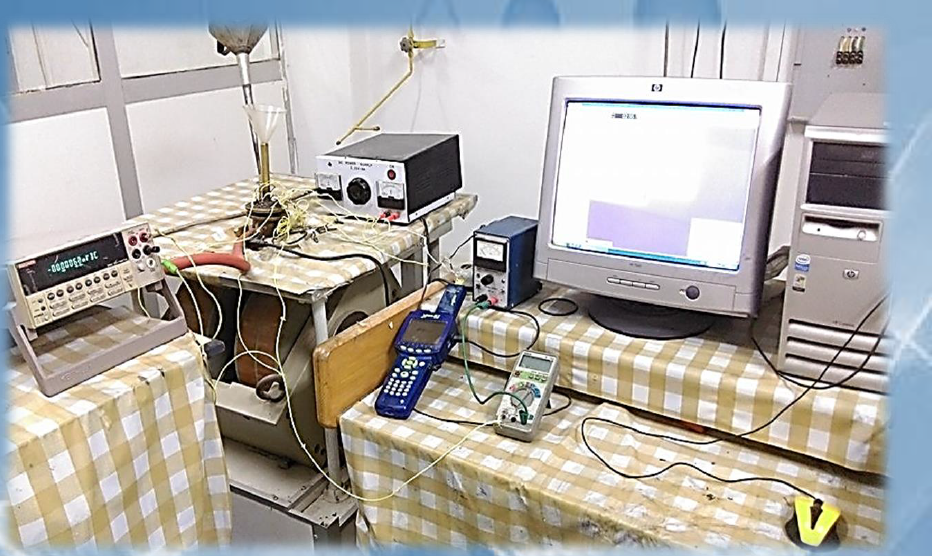
Van der-Pauw Circuit
Model
custom/laboratory built
Units Available
1
Manufacture Year
2010
Manufacturer Website
Description
The Van der Pauw circuit is used for precise measurement of resistivity, sheet resistance, and Hall effect parameters of thin films and semiconductor samples with arbitrary shapes. Using four-point contact geometry, the Van der Pauw method allows determination of sheet resistance, carrier concentration, and carrier mobility without assuming a specific sample shape, as long as the sample is homogeneous and has a uniform thickness. The circuit typically includes: Four electrical contacts (probes) on the sample corners Switchable current sources and voltage measurement channels Integration with a magnetic field for Hall effect measurements Data acquisition system for automatic calculation of resistivity and Hall coefficient Applications include semiconductor characterization, thin film studies, and electronic materials research.
Services & Pricing
| Service | Cost |
|---|---|
| 0 | - |
Additional Information
Measurement Principle: Four-point probe technique for resistivity and Hall effect measurements using Van der Pauw geometry. Sample Requirements: Thin, flat, homogeneous samples with uniform thickness; electrical contacts must be small and well-defined. In